NIRISS Detector Performance
Various fundamental properties of the JWST NIRISS detector that affect the overall science performance were measured in ground testing in late 2015 and early 2016 and verified in-flight during commissioning and science operations.
On this page
See also: NIRISS Detector Readout, NIRISS Detector Readout Patterns
The NIRISS detector is a 2048 × 2048 HAWAII-2RG device with a wavelength cut-off around 5 μm, in the same "family" of detectors as the 2 NIRSpec detectors and the 2 guider detectors. It is also similar to the NIRCam long wavelength devices.
The NIRISS detector and the application-specific integrated circuit (ASIC) were tested in flight-like configuration during the Integrated Science Instrument Model (ISIM) cryo-vaccum test 3 (CV3), which took place between November 2015 and February 2016. Performance was then verified during NIRISS commissioning using in-flight data.
Various detector properties are observed to be different in the epoxy voids, which cover about 20% of the total detector area. Where possible, values are given for the void regions and for the main area of the detector. The values reported here reflect in-flight performance measured during commissioning.
Summary table
Words in bold are GUI menus/
panels or data software packages;
bold italics are buttons in GUI
tools or package parameters.
Table 1. In-flight values at a NIRISS operating temperature of 39 K
| Quantity | Value | Value in the void (if applicable) |
|---|---|---|
| Read noise (correlated double sampling) | 16.8 e- | |
| Total noise | 10.3 e– for a 120 group NISRAPID integration | |
| Gain | 1.61 e–/ADU | |
| Inter-pixel capacitance | 0.44% to each row/column adjacent pixel | 0.22% to each row/column adjacent pixel |
| Dark signal | 0.515 e-/frame | 0.279 e-/frame |
| Full well capacity | 95,000 to 105,000 e– |
Further details are given below.
Read noise
Measurements of the read noise were derived from taking correlated double sample (CDS) images from long dark integrations and finding the average dispersion about zero. This measurement includes the read noise as well as some contribution from the 1/f noise and a small contribution from the dark signal, although the measured value is expected to be dominated by uncorrelated 1/f noise and the read noise. The average value of the CDS read noise was found to be 16.8 e-. These values are for raw integrations before the reference pixel correction. The read noise per frame is therefore the CDS read noise value divided by √2.
Total noise
Figure 1 shows the total noise as a function of the number of groups in an integration, for up to 120 groups in NISRAPID readout (a total exposure time of 1299.15 s). This analysis was done using in-flight data from commissioning at the NIRISS operating temperature of 39 K. The "read noise" is determined by removing the dark signal component from the total noise, but this value includes read noise and 1/f noise. Hence the "read noise" values so obtained are somewhat larger than the read noise value determined from the CDS frame analysis given above.
Figure 1. Total noise for NIRISS detector as a function of integration time

The derived total noise of the NIRISS detector from darks observations taken during commissioning. The total noise includes the read noise, 1/f noise, and the dark current component. The curve labeled "read noise" is the total noise minus the estimated dark current contribution, and so it includes both read noise and the 1/f noise.
Gain
The NIRISS detector gain was measured with the photon transfer method in a large set of integrations with close to uniform illumination during CV3 testing. The average gain value was found to be 1.61 e–/ADU, with roughly a 10% uncertainty. The gain value has been corrected for the inter-pixel capacitance (IPC) effects. As the IPC is smaller in the voids, the raw measured gain before correction is slightly larger in the voids than outside the voids. However the net gain after the correction appears to be the same inside and outside of the voids.
Dark signal
Analysis of the NIRISS dark ramps taken in different subarray configurations shows that the signal per frame in the dark exposures is nearly constant for different frame read times, ranging from 0.07544 s for the SUB80 subarray to 10.73677 s for the full frame read-out. This behaviour is attributed to a signal from the back-plane electronics associated with reading out each pixel. The actual dark current is too small to measure accurately when this other signal is present. For this reason, the dark signal is given electrons/frame rather than a dark current value in electron/s.The average dark signal measured from commissioning data was 0.279 e-/frame in the voids and 0.515 e-/frame for the rest of the detector. Figure 2 shows the dark signal across the NIRISS detector.
Figure 2. Dark signal across the NIRISS detector
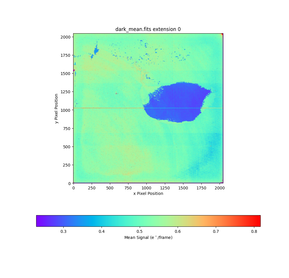
The areas of low dark signal are the epoxy voids. There are many small voids in channel 1 and a single large void, in channels 2 and 3, on the right.
Figure 3. Clipped mean and median dark signal values for different calibration dark ramps
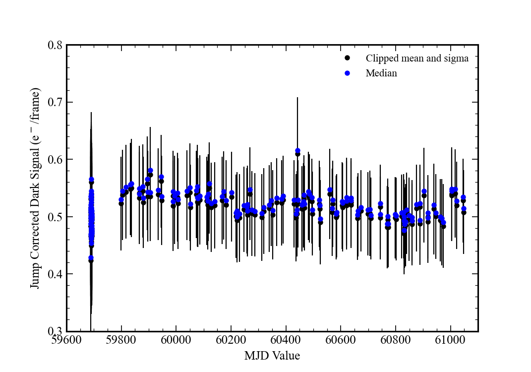
The clipped mean/median dark signal from the NIRISS dark calibration observations, where the dark signal values have been corrected for jumps in Stage 1 of the pipeline. The blue points are the median values for each observation. The black points are the mean values with the standard deviation shown as the error bars. The high point just above 0.6 electrons/frame was due to a solar storm that affected one of the dark calibration observations.
Inter-pixel capacitance
The inter-pixel capacitance (IPC) was measured from isolated hot pixels or cosmic ray hits in the CV3 dark ramps. Averaging over many such pixels, the IPC effect appears to be symmetric from the central pixel to the 4 adjacent pixels along the row or column. The average magnitude of the coupling is 0.22% (per pixel, so 4 times this overall) in the voids and 0.44% outside the voids.
The post-pixel coupling adds about 0.15% to the signal observed in the pixel next along in the read direction. Thus the "raw" IPC values show an asymmetry in the read direction that differs between channels 1 and 3 and channels 2 and 4 of the detector.
Detector full well capacity
The detector full well capacity was measured in the detector testing at Teledyne Imaging Sensors prior to delivery. The general full well depth is about 105,000 e–. With the gain setting selected for flight the full well capacity is not reached for some pixels because they pass the A/D conversion limit of 65,535 ADU before the full well depth. About half of the detector pixels are subject to A/D saturation and the other half reach full well before A/D saturation, typically between 95,000 and 105,000 e–. Due to the non-linearity effects, the raw full well value in raw ADU is generally in the range between 60,000 and 65,535 ADU. After subtraction of the pedestal, the saturation values range from 42,000 ADU to 57,000 ADU as there is significant structure in the pedestal.
When 2 neighboring pixels accumulate charge at very different rates, the brighter pixel "spills" photoelectrons to its neighboring pixels, but the reverse effect does not occur. This charge migration causes the full width half maximum (FWHM) of the point spread function (PSF) to be larger for bright point sources compared to faint point sources (the so-called"brighter-fatter effect"). For the NIRISS detector, charge migration starts at a signal limit of ~23,300 e- (though the actual limit depends on filter), so some observers, especially those using the NIRISS aperture masking interferometry mode, may wish to design programs to stay below this limit.
References
Hirata, C. M., Choi, A. 2019, PASP 132, 1007 (ADS)
Brighter-fatter effect in near-infrared detectors – I. Theory of flat auto-correlations